

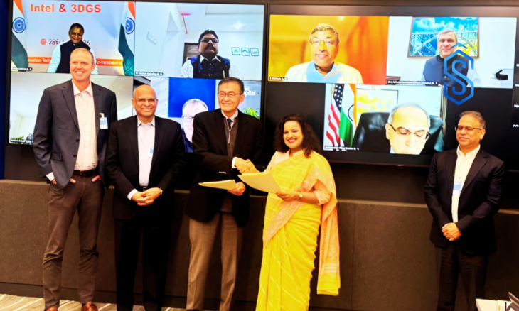
New Delhi: In a significant development for India’s semiconductor ambitions, substrate manufacturing is set to receive a major boost following the signing of a landmark Memorandum of Understanding (MoU) between the Government of Odisha, Intel Corporation, and 3DGS Inc., USA.
The agreement aims to establish an Advanced Packaging Glass Core Substrate Manufacturing Facility in Odisha, marking one of the largest high-technology manufacturing investments in the country.
Union Minister of Electronics & Information Technology Ashwini Vaishnaw, along with Odisha Chief Minister Mohan Charan Majhi, Intel CEO Lip-Bu Tan, and other dignitaries, witnessed the signing of the MoU to bring advanced substrate manufacturing technology to India.
The MoU provides a framework for setting up an Advanced Packaging Glass Core Substrate Manufacturing Facility in Odisha.
The proposed facility is planned for the Bhubaneswar–Khurda region and is expected to play a pivotal role in strengthening India’s substrate manufacturing ecosystem and semiconductor value chain.
Also Read: Future of India’s Semiconductor Industry Roadmap Targets $150 Billion Value Chain by 2035
Speaking on the occasion, Ashwini Vaishnaw emphasized that the signing of the landmark MoU aligns with the Government of India’s vision of developing the entire semiconductor manufacturing ecosystem.
He noted that investments and partnerships involving leading global technology companies reflect growing confidence in India’s semiconductor sector and reinforce the country’s position as an emerging destination for advanced substrate manufacturing.
The Union Minister stated that the entry of global firms such as Applied Materials Inc., Lam Research, Tokyo Electron Ltd., and Merck Electronics, along with the MoU signed between Tata Electronics and Dutch multinational ASML, serves as recognition of the government’s efforts to strengthen the semiconductor industry and demonstrates the trust international players place in India.
The proposed substrate manufacturing project is expected to be implemented in phases over a period of five to six years.
Upon completion, it is anticipated to generate substantial direct high-skilled employment opportunities while also creating significant indirect jobs across the broader manufacturing, technology, and supply-chain ecosystem.
The facility will focus on advanced packaging glass core substrates, high-density interconnect substrates, and related semiconductor technologies.
Intel will support the initiative through technology know-how and process expertise, helping to advance India’s capabilities in substrate manufacturing and semiconductor packaging technologies.
Officials highlighted that the project is expected to contribute significantly to capability development, ecosystem growth, and export-oriented manufacturing.
The establishment of such a facility is expected to further strengthen India’s position in the global semiconductor industry while accelerating domestic substrate manufacturing capabilities.
Also Read: E-Mobility Center of Excellence Bridges Academia and EV Industry at MIT-WPU
The initiative builds upon ongoing efforts under the India Semiconductor Mission, which seeks to strengthen domestic manufacturing, enhance semiconductor design capabilities, and develop resilient supply chains.
By bringing advanced substrate manufacturing technology to the country, the project is expected to support India’s long-term semiconductor strategy and industrial growth objectives.
The proposed facility is also expected to position Odisha as a key destination for semiconductor investments and digital infrastructure development.
With the establishment of advanced substrate manufacturing capabilities, Odisha could emerge as an important node in the global semiconductor ecosystem while contributing to India’s broader technology and manufacturing ambitions.