
India has made significant progress toward its ambitious goal of training 85,000 semiconductor engineers under the Government of India’s Chips to Startups (C2S) initiative, part of the India Semiconductor Mission (ISM).
The program focuses on talent development through training, upskilling, and workforce development to strengthen the country’s semiconductor ecosystem.
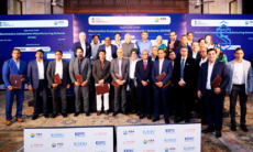
Union Minister for Railways, Information & Broadcasting, and Electronics & IT, Ashwini Vaishnaw, said India has made notable progress over the last four years toward achieving its 10-year target of developing a large pool of semiconductor engineers skilled in chip design and related technologies.
Also Read: India Semiconductor Mission 2.0 Announced to Boost Manufacturing, IP, and Supply Chains
Speaking about the initiative, Vaishnaw highlighted that world-class Electronic Design Automation (EDA) tools supported by leading technology companies such as Synopsys, Cadence Design Systems, Siemens, Renesas Electronics, Ansys and AMD have been deployed across 315 academic institutions in India.
These advanced platforms are enabling students to gain hands-on training and practical exposure as semiconductor engineers.
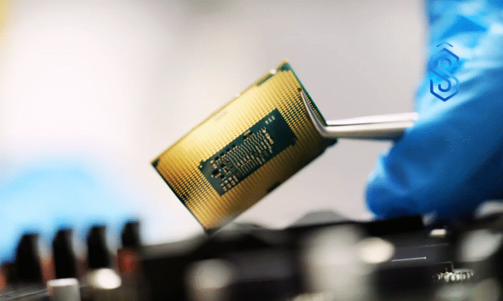
With access to these EDA tools, students are designing semiconductor chips as part of their academic learning. The chips designed by aspiring semiconductor engineers are fabricated and tested at the Semiconductor Laboratory (SCL) Mohali, allowing them to experience the entire semiconductor lifecycle – from design and fabrication to packaging and testing.
According to the government, the initiative has grown into the world’s largest open-access EDA programme for semiconductor engineers, with more than 1.85 crore hours of EDA tool usage already recorded for chip design training. The usage continues to grow as more students participate in semiconductor development programs.
Also Read: C2i Semiconductors Raises $15 Million Series A Led by Peak XV Partners
Semiconductor Engineers: Sector Requires Nearly Two Million Skilled Professionals
Vaishnaw further stated that students from academic institutions across the country—from Assam to Gujarat and from Kashmir to Kanyakumari—are actively participating in semiconductor design activities.
This widespread engagement reflects the growing interest in semiconductor technology and the increasing pipeline of future semiconductor engineers across India.
The minister emphasized that as the global semiconductor industry expands from its current size of approximately USD 800–900 billion to an estimated USD 2 trillion, the sector will require nearly two million skilled professionals.
This projected growth creates vast employment opportunities for Indian youth aspiring to become semiconductor engineers.
To further strengthen the talent ecosystem, Vaishnaw announced that under India Semiconductor Mission 2.0, the Chips to Startups programme will expand from 315 academic institutions to 500 institutions nationwide.
This expansion aims to ensure that more students can develop skills required to become semiconductor engineers across fields such as semiconductor design, fabrication, packaging, and testing.
Reiterating the government’s long-term vision, the minister said the Government of India remains committed to building a strong and self-reliant semiconductor ecosystem.
Through talent development, infrastructure creation, and industry collaboration under the India Semiconductor Mission 2.0, the country aims to establish itself as a global hub for semiconductor engineers and semiconductor innovation.